
The European Union has announced a 525 million euro support plan and the launch of a European chip design platform to expand the semiconductor design ecosystem. The point is that we will not only focus on building a new semiconductor factory, but also increase the number of companies that plan and design the chips to be produced at that factory.
The European Commission explained that European semiconductor design companies account for less than 1% of global market sales. Even if the factory is increased, if there are not enough design companies to order locally, the production base and industrial ecosystem can move separately.
The European Chip Design Platform, which was announced this time, is a structure that helps startups and SMEs secure expensive design software, design assets, technical support, and access to manufacturing facilities. However, this does not mean that the total amount of the plan has already been paid to all participating companies or that all support services are immediately complete.
| The composition of the 525 million euro plan

The total amount of support announced is 525 million euros. According to Reuters, the European Commission and its member states invested 440 million euros in supporting the development of commercial chips and proposed a structure that supports the European chip design platform with 85 million euros separately. It's an approach to organize development costs and common support infrastructure together.
Just because the amount is large does not mean that one company or all kinds of semiconductors are put into it. The actual beneficiaries of various support projects vary depending on the target, the selection process, and the execution period. What is currently confirmed is the size of the policy and the announcement of the launch of the platform, so it is difficult to write that we have already confirmed the completion of the payment or the business performance for individual companies.
| Bottleneck in the design phase ahead of the production facility

The semiconductor supply chain leads to planning the chip structure and designing the circuitry, validating the design, and producing and packaging it in the factory. Design companies do not have to directly own a manufacturing facility to determine the function and performance of the product. These companies are often called fabless.
Europe has important companies in the automotive, industrial equipment, and power semiconductor sectors, but they do not have the same competitiveness in all areas of chip design. The indicator that the share of global design market sales is less than 1% presented by the Executive Committee is the starting point for the policy judgment that the design capacity in Europe should be further increased. However, since it is a statistic according to the market definition, it does not mean that the total semiconductor manufacturing capacity in Europe is less than 1%.
| The role of cloud-based design platforms

The European Chip Design Platform is a window for various design companies to utilize the tools they need in common. Semiconductor development requires electronic design automation software, i.e., EDA tools, and verified IP blocks and professional design support services are also important. It takes a high cost and time for an early-stage company to contract and maintain each and every one of these.
The public platform is designed to lower this barrier to entry. The Executive Committee presented key services such as design tools, design support, IP blocks, training and funding connections, and access to manufacturing facilities. In practice, it is important to qualify for access by service, structure of costs, and timing of provision. It is necessary to distinguish between the platform launch itself and the full commercial operation of each function.
| Burden of chip design assets and initial development costs
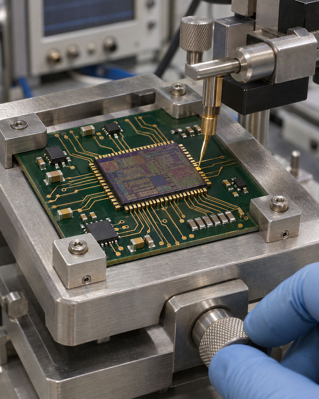
Semiconductor chips cannot be sold by design alone. Several costs are incurred, such as verification, prototyping, and modification tailored to the mass production process, and the cost of funds is increased if the design is redesigned by mistake. For startups, it's a barrier to determining whether the upfront costs of design software usage or trial production can sustain the business.
With proven IP blocks, you don't have to design everything from scratch. As the connection with the manufacturing facility becomes easier, the possibility of initial prototype verification increases. However, a common service does not guarantee success. This is because it is a commercial product only when the performance desired by the customer is secured and the price and delivery conditions are met.
| EU Semiconductor Law and Technology Sovereignty Strategy

The plan is an extension of the policy under the EU Chips Act. Europe's semiconductor policy has emphasized production capacity and supply chain stability, but if the pool of design companies is not expanded, new production facilities can also rely on overseas customers' orders. That's why we want to strengthen the connection within the region from design to manufacturing.
The EU's technological sovereignty is closer to securing the option to design and procure key technologies rather than severing all dealings with other regions. In the face of stronger industrial policies from the United States and China, it can be interpreted as a move by Europe to increase its own product planning and professional workforce. However, the dependence on offshore technology and equipment does not disappear at once.
| AI Semiconductor Market and Startup Opportunities
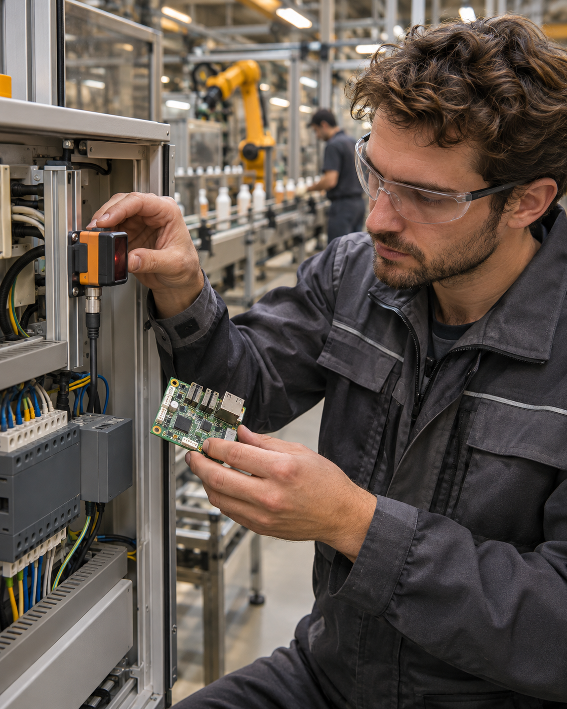
As the AI market grows, not only accelerators for data centers, but also power management, network connectivity, sensor processing, and inference chips in industrial sites are showing up in demand for various products. Competing directly with the leaders in the large general-purpose GPU market is not the only option for design startups. Professional chips that optimize performance and power consumption in narrow applications can also be a business opportunity.
Industrial customers and research institutes that already exist in Europe are based on connecting new chip ideas to real-world problems. However, promising research results do not guarantee sales soon. After a startup creates a prototype, the key is to be able to continue with quality certification, design modification, customer acquisition, and stable production contracts.
| Metrics to determine the effectiveness of a support policy

Follow-up metrics are more important than the presentation budget to see if the policy actually works. We need to check the number of design companies selected, the actual utilization rate of design tools, the number of prototypes manufactured, products that have been successfully commercialized, and private capital attraction and sustainable sales. There can be a considerable time lag between announcing policies and improving corporate competitiveness.
Providing access to manufacturing facilities does not always guarantee free capacity. The difference between fleet access, packaging, production yield, intellectual property protection, and country-specific support standards remains. I need to verify that the platform has lowered the actual development period and cost beyond a simple guide window.
| The long-term challenge of expanding the design ecosystem
The significance of this launch is that Europe has expanded the center of its semiconductor policy not only to expand manufacturing facilities but also to foster design companies. When the idea of making technology tools, funding, and manufacturing connections accessible in one place becomes a reality, even small businesses can be prone to taking the first step in product development.
In the future, we need to see how development support of 440 million euros and platform support of 85 million euros are executed, which companies are selected, and whether private customer orders are actually growing. Mass production and export of designed products are more important than the announced amount. The self-reliance of the European semiconductor industry will be revealed in the accumulation of its performance rather than a short-term declaration.
Tags
#EU #European Union # Semiconductor Policy #EUChipsAct #Semiconductor Design Fabless #EDA #SemiconductorStartup #Technological Sovereignty # Chip design platform #Industrial Policy