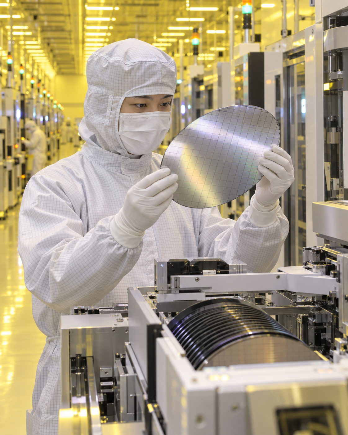
CXMT, China's largest DRAM manufacturer, announced that it has begun mass production using its fifth-generation technology platform. The company stated that it has reduced the pitch of the core memory structure to 11.95 nanometers and that it is already mass-producing two 24Gb LPDDR5X products based on the same platform.
The most striking figure in this announcement is that compared to the previous 4th-generation platform, The total number of chip dies that can be produced from a single wafer has increased by at least 50%. However, this figure does not represent the yield—the percentage of chips that pass the final inspection—but rather the total number of dies that can be obtained from a wafer before defective ones are sorted out.
Whether CXMT's announcement will lead to an actual increase in supply and price competition can only be determined once customer certification, yield rates, and production volumes are confirmed. Still, given that a Chinese company has announced it has brought both advanced process technology and high-capacity mobile DRAM into mass production simultaneously, this can be seen as an event that demonstrates the pace at which China is catching up in a market long dominated by Samsung Electronics, SK Hynix, and Micron.
| 5th-generation platform featuring a 11.95-nanometer pitch
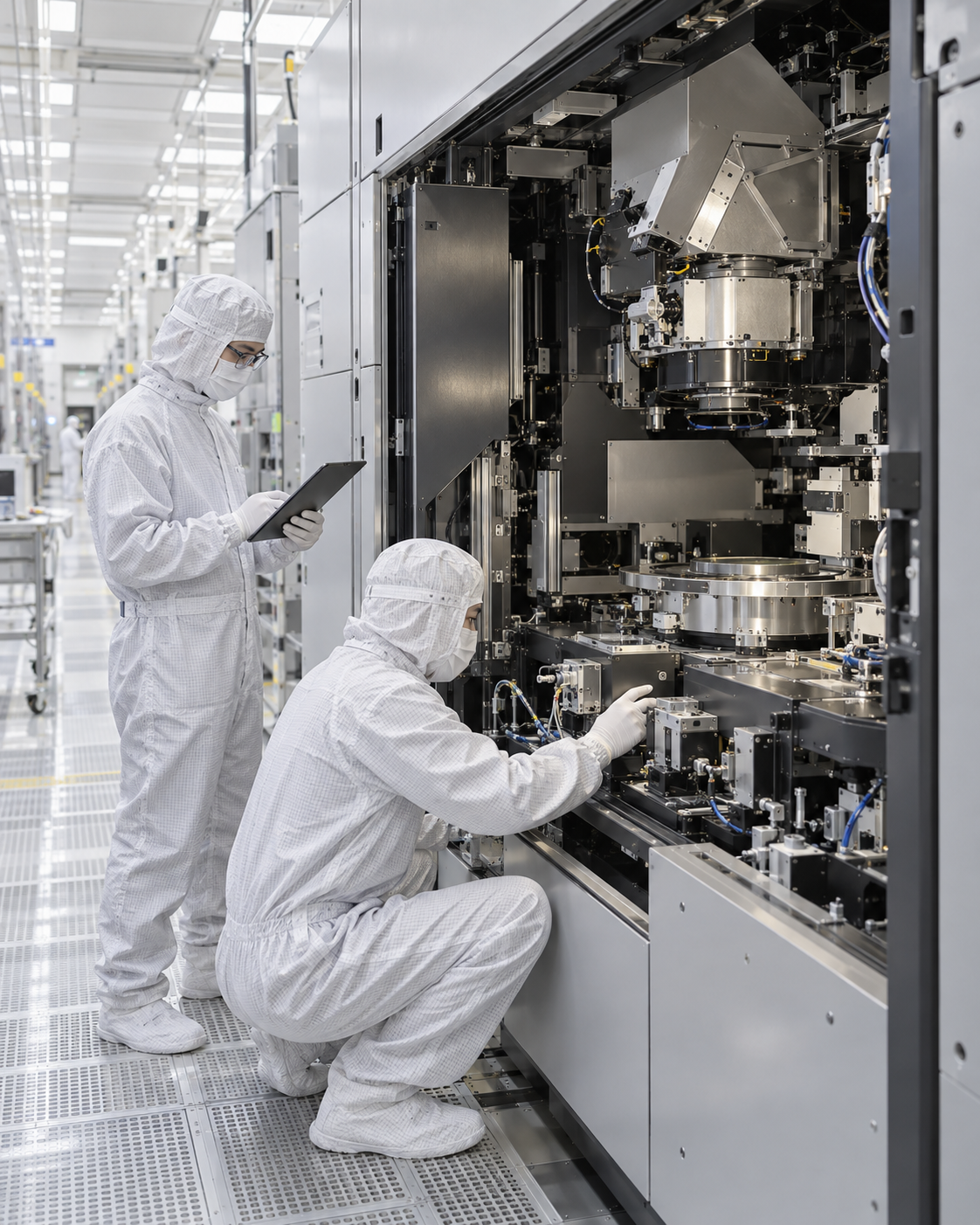
At the 2026 World Manufacturing Conference, CXMT announced that its fifth-generation DRAM technology platform had entered mass production. DRAM is a type of working memory that temporarily stores data being processed by smartphones and PCs; to store more information within the same area, the core structures surrounding the cells must be made denser.
The company explained that it had reduced the pitch of the core structure in the data storage unit to 11.95 nanometers. This process utilized quadruple patterning technology, which involves repeating the same patterning process multiple times to create finer circuits.
CXMT claims that its process capabilities have reached a level comparable to the industry's most advanced mass-production nodes. However, this is the company's own assessment, and this announcement did not include independent performance, power consumption, or yield data obtained from comparisons with competing products under the same conditions.
| A 50% increase per wafer is a different metric from yield.
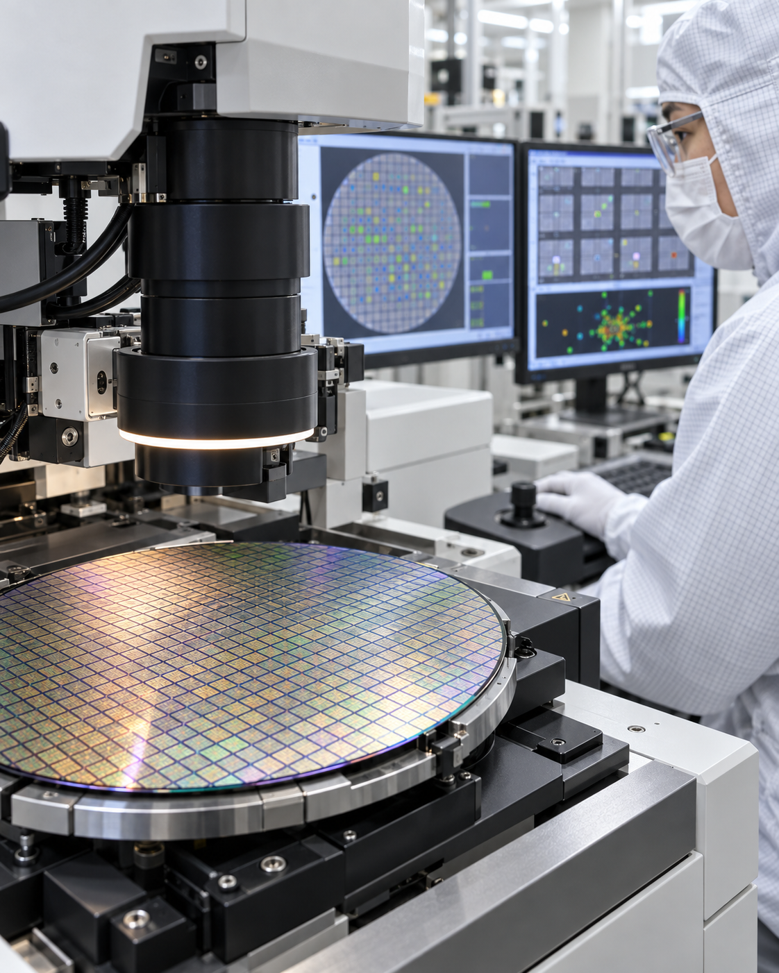
CXMT stated that, based on 8Gb chips, the total number of dies per wafer on the new platform has increased by at least 50% compared to the fourth generation. As circuit sizes shrink, more chips can be placed on a single round silicon wafer, which theoretically creates an opportunity to lower the manufacturing cost per chip.
Here, the total number of dies refers to the number of chips placed on the wafer prior to the final inspection. To determine the actual number of chips that can be sold, you need to consider the yield—the percentage of chips that function properly—as well. Therefore, a 50% increase should not be interpreted to mean that the output of finished products or sales will immediately rise by 50%.
The key issue to monitor going forward is how quickly production scale can be expanded while maintaining a stable yield. Quadruple patterning, which involves an increased number of process steps, helps enable the fabrication of fine circuits, but it can also increase process time and the complexity of equipment operation.
| Both 24Gb LPDDR5X products are currently in mass production.
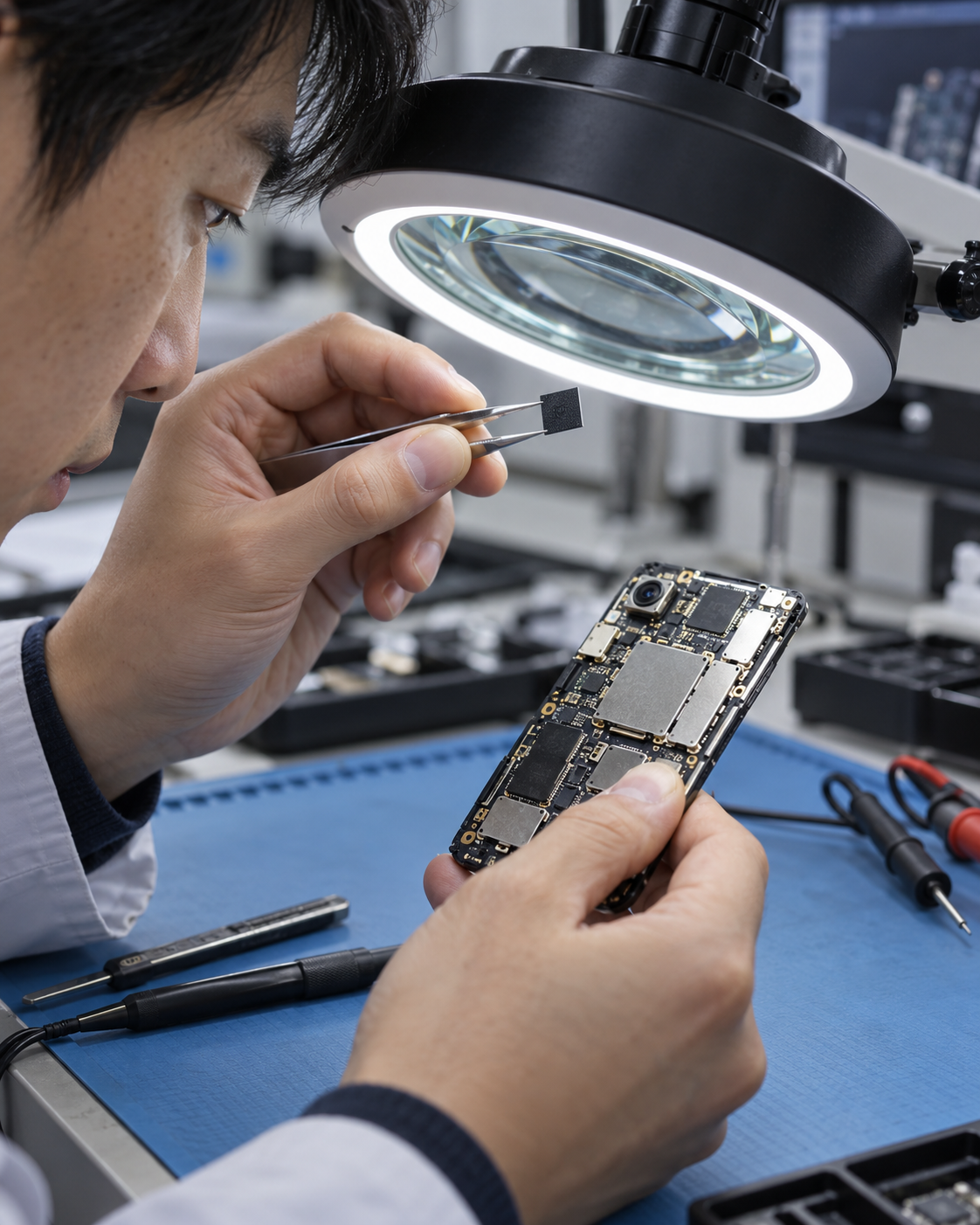
CXMT also unveiled two 24Gb LPDDR5X products built on its new platform. The two products feature different package formats to accommodate various smartphone and mobile device designs, and according to the company, they offer 50% more storage capacity than existing products in the same class.
LPDDR5X is a low-power DRAM primarily used in battery-powered devices such as smartphones and tablets. As the capacity of a single chip increases, manufacturers can achieve the same memory capacity using fewer chips or increase the total memory capacity within the device’s limited internal space.
However, this announcement alone does not provide details on the actual product's data transfer speed, power consumption, heat generation, or adoption status among customers. Although the 24Gb capacity and mass production status have been confirmed, specific part numbers and certification results are still needed to assess its market competitiveness.
| A Process Developed in Collaboration with China's Equipment Ecosystem

CXMT explained that it developed the new platform by utilizing computer simulations and collaborating with Chinese equipment manufacturers during key production stages. Given the ongoing U.S. export restrictions on advanced semiconductor equipment and software, the fact that the company leveraged local supply chains is what gives this announcement its industrial significance.
The DRAM manufacturing process cannot be completed with just one lithography system. Since it requires a series of interconnected steps—including deposition, etching, cleaning, measurement, defect inspection, and process control—joint development with local equipment manufacturers could also contribute to the accumulation of experience across the entire Chinese semiconductor ecosystem.
That said, it’s hard to say that our dependence on foreign equipment and technology has completely disappeared. That's because this announcement did not disclose the localization rates for each type of production equipment or the procurement structure for key materials.
| Pressure on the Top 3 Existing Memory Manufacturers

The global DRAM market is led by Samsung Electronics, SK Hynix, and Micron. If CXMT expands its supply of high-capacity mobile DRAM, procurement options—particularly for Chinese smartphone manufacturers—will increase, and price competition for general-purpose products could become even more intense.
In contrast, leading companies are focusing their investments on areas that are both technically challenging and highly profitable, such as high-bandwidth memory (HBM) and high-performance DDR products for servers. While CXMT's latest announcement demonstrates its production competitiveness in mobile DRAM, it does not mean that the overall technology gap has been closed.
The actual impact on the market is likely to be reflected in the adoption rates and shipment volumes of major smartphone manufacturers. Long-term supply contracts, customer certifications, and quarterly production volumes will be more important indicators than product announcements.
| Three Things to Watch for After the Yangsan Declaration
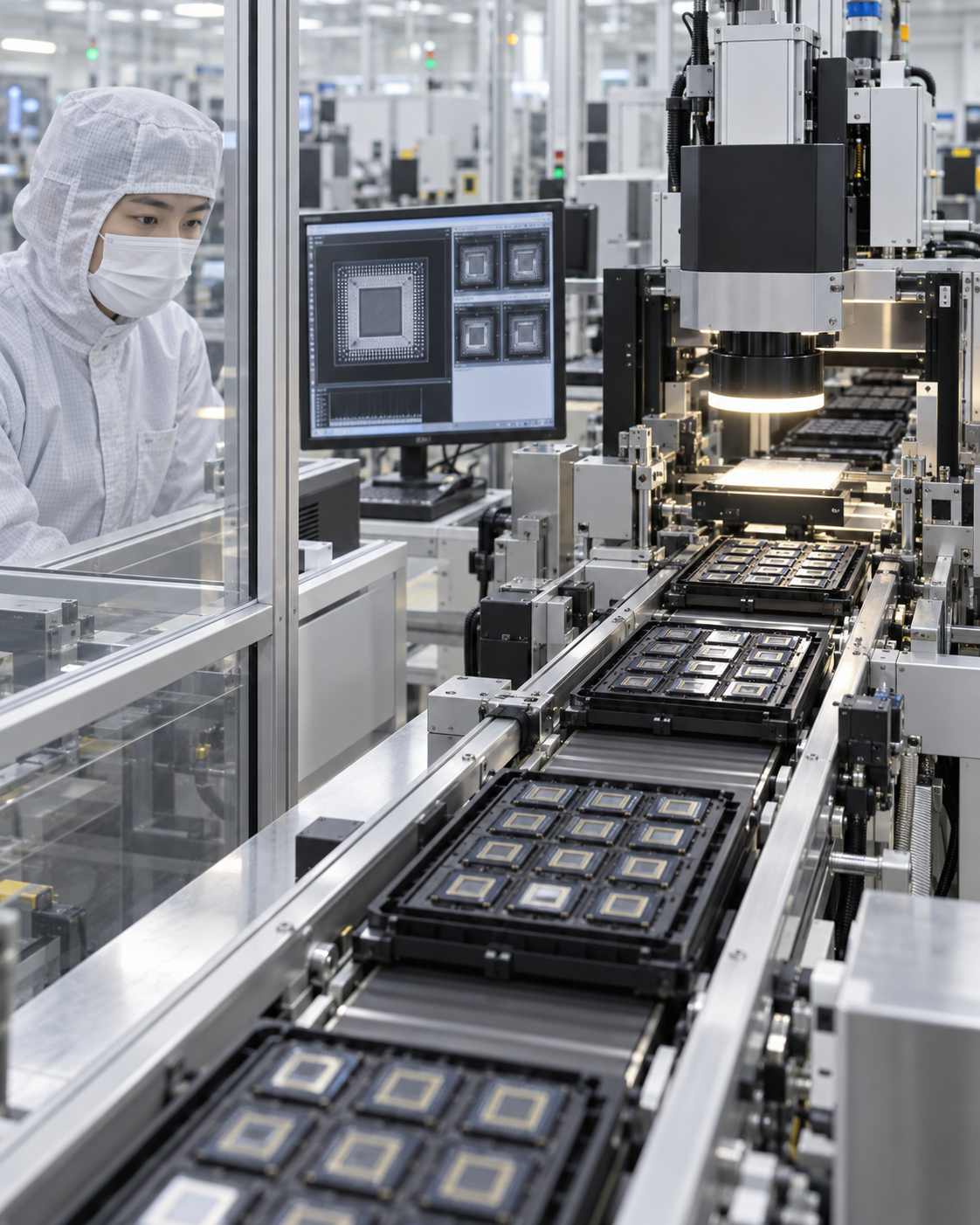
According to the company's official statement, the announcement confirmed that two products—the 5th-generation platform and 24Gb LPDDR5X—have entered mass production. The company also confirmed figures showing a core feature size of 11.95 nanometers and a minimum 50% increase in the total number of dies per wafer.
The aspects that have yet to be verified are the final yield, monthly production volume, actual power consumption and speed, and the scale of adoption by customers. In particular, we need to distinguish between the increase in the total number of dies per wafer and the increase in the number of saleable, defect-free dies.
Going forward, we'll need to see if specific product specifications, customer certifications, actual devices featuring the product, and stable shipment volumes are disclosed. These indicators must follow in order to properly assess the impact of CXMT’s process progress on the global DRAM supply structure and prices.
Tags
#CXMT #Changsin Memory #DRAM #LPDDR5X #24Gb Memory #Chinese Semiconductors #Memory Semiconductors #Semiconductor Processes #Quadruple Patterning #SmartphoneMemory #Wafer #Semiconductor Infrastructure