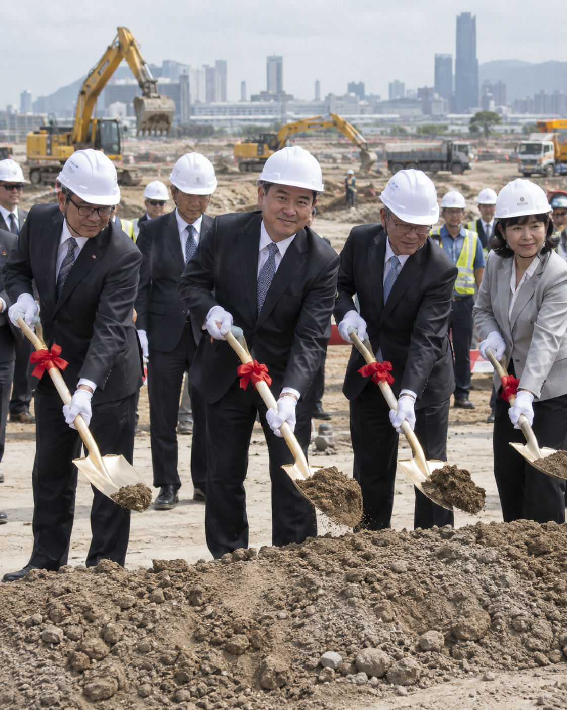
Taiwan has begun developing the Baipu Industrial Park in Kaohsiung, in southern Taiwan, which is aimed at establishing a semiconductor supply chain for AI and high-performance computing. At the heart of this project are a technology verification laboratory and a talent training center to be built by TSMC. The goal is for both facilities to begin operations in the fourth quarter of 2029.
This complex is different in nature from projects that simply expand the number of factories directly mass-producing semiconductors. The key is to bring together in one place a space where equipment and materials companies can research, test, and validate technologies for use in TSMC’s cutting-edge packaging processes. The goal is to reduce the time it takes for technologies in the research phase to move into actual mass production.
However, as of September 21, 2026, the only confirmed details are the groundbreaking for the industrial complex, TSMC’s plans to build two facilities, and the target to begin operations in the fourth quarter of 2029. The specific list of tenant companies, their production capacities, detailed investment amounts, and the scope of packaging technologies to be validated have not yet been disclosed.
| A verification hub will be established on an 88.7-hectare site
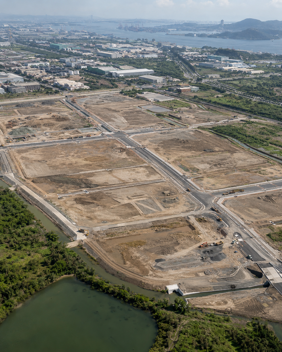
The Baipu Industrial Park has a total area of approximately 88.7 hectares, of which about 53.6 hectares are scheduled to be designated as industrial land. It is reported that the Kaohsiung City Government will construct the factory facilities, while TSMC will occupy two buildings within the park.
The facilities TSMC will build are a technology validation lab and a training center. The technology validation lab will be responsible for verifying that equipment and materials meet the requirements of actual cutting-edge packaging processes, while the training center is expected to serve as a foundation for developing personnel capable of handling related processes and equipment.
That doesn't mean the entire industrial complex is a TSMC manufacturing plant. By combining TSMC facilities with spaces for supply chain companies, it is becoming more of an industrial ecosystem hub that supports research, testing, and education.
| Why Advanced Packaging Has Emerged as a Bottleneck for AI Semiconductors
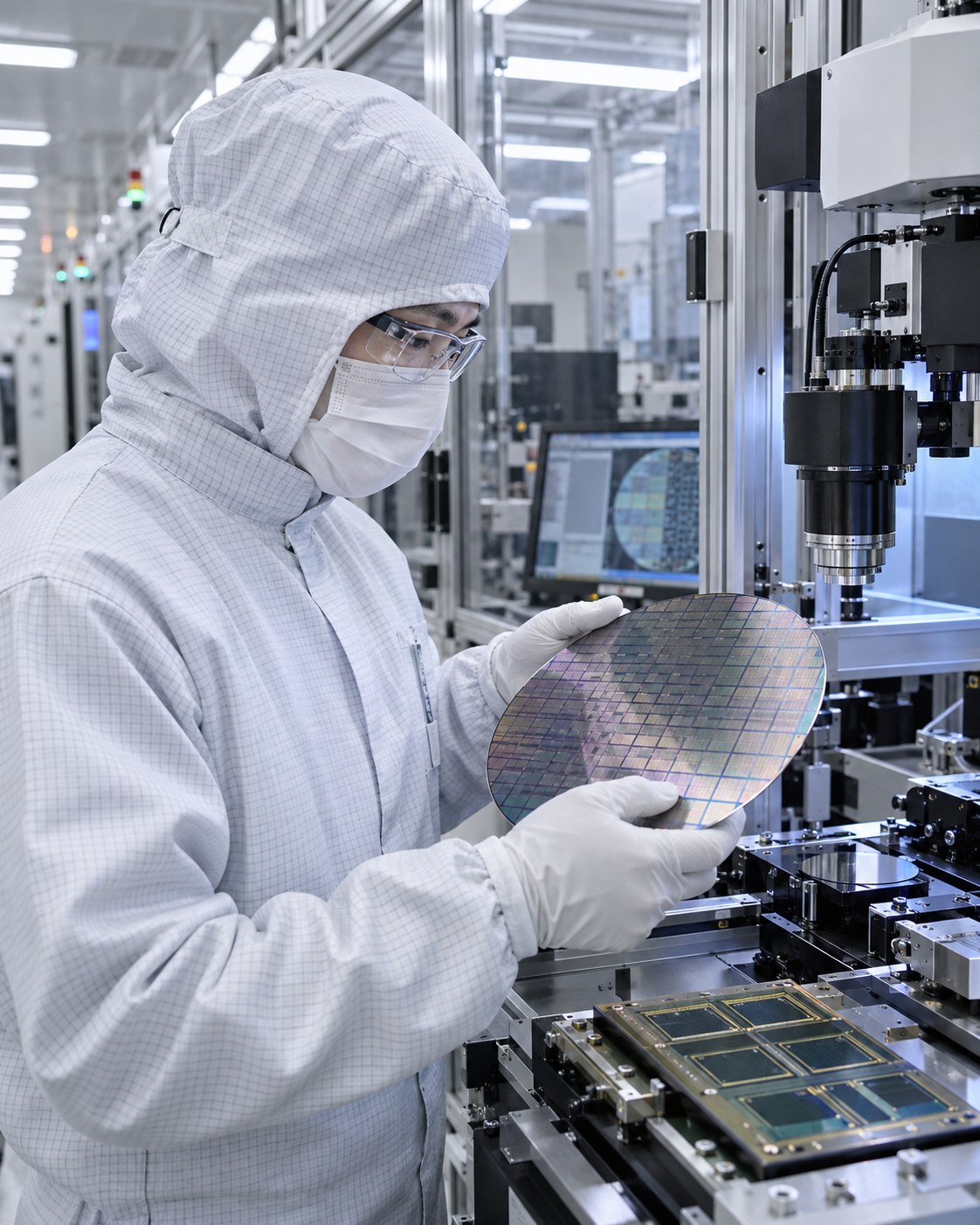
Advanced packaging isn't just the final packaging step that protects the finished chip from external impacts. It's a technology that connects multiple chips—such as processing chips and high-bandwidth memory—over short distances and enables them to function as a single system. It influences everything from the speed of data transfer between chips to power efficiency and thermal management.
Since AI accelerators require the rapid exchange of large amounts of data, packaging capabilities have become just as important as advanced process technology. TSMC’s cutting-edge packaging technology is also being utilized in high-performance AI chips designed by companies such as Nvidia, AMD, and Broadcom. As demand grows, a stable supply of packaging equipment, substrates, materials, and inspection and measurement technologies will also be essential.
The Baipu complex can be viewed as an investment aimed at reducing the time required to validate equipment and materials within this supply chain. Even if a new technology is successful in the lab, repeated testing is necessary to ensure yield and reliability on actual mass production lines; having verification facilities and suppliers nearby can speed up collaboration.
| This presents an opportunity for suppliers to lower barriers to entry
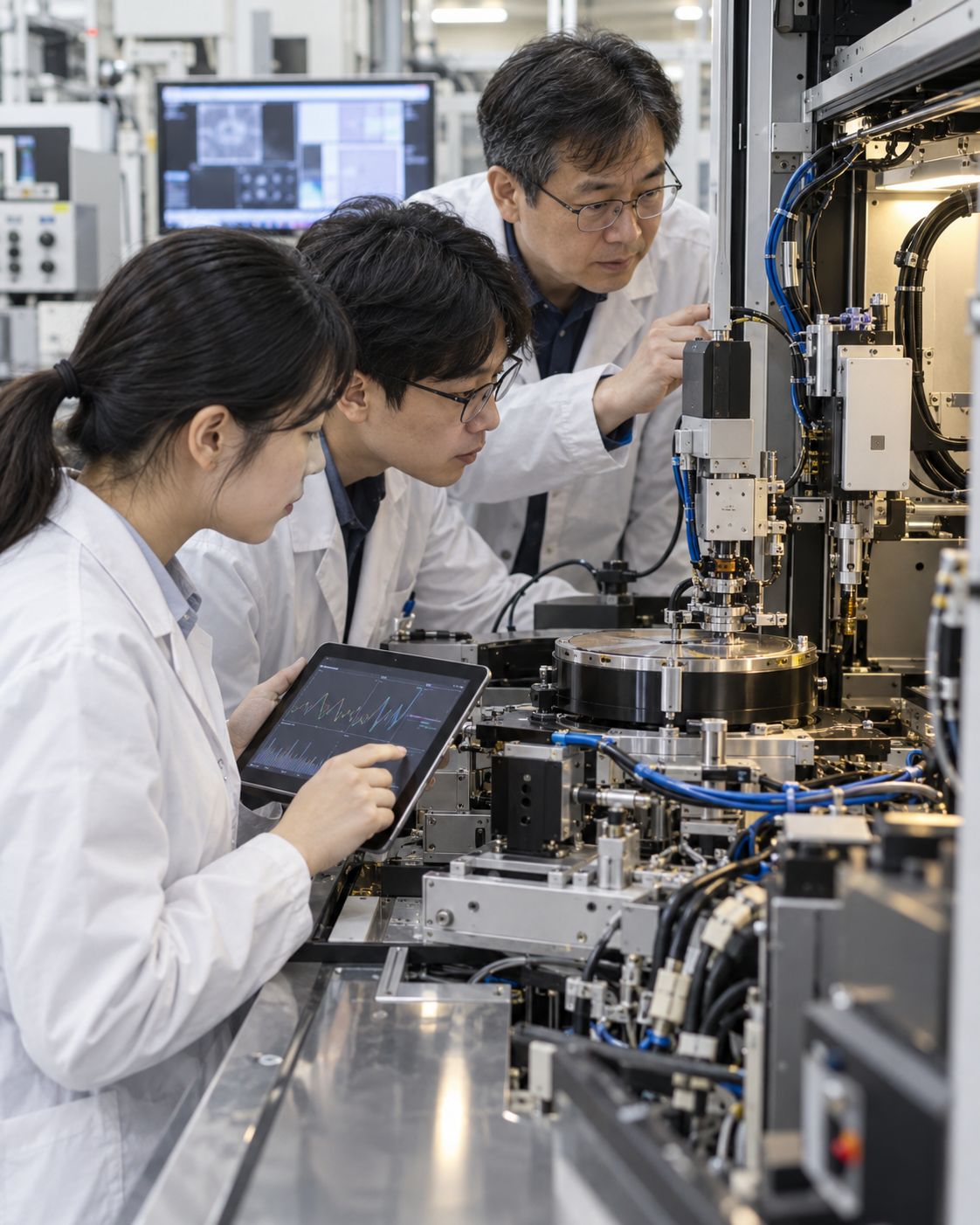
Semiconductor equipment and materials cannot be immediately incorporated into mass production lines simply because they appear to perform well. Even minute contamination or process variations can affect yield, so long-term validation tailored to the customer’s specifications is required. For regional companies that lack access to the validation systems of major semiconductor firms, this process itself can serve as a significant barrier to entry.
The Taiwanese government explained that if suppliers conduct research, testing, and validation at Baipu, it will shorten the time required to transition new technologies to mass production and help local companies enter the supply chain. This means creating a structure where customers and suppliers can quickly exchange test results within the same region, rather than simply providing a site.
However, just because a verification center is established doesn't mean every company will automatically secure a supply contract. Actual results depend on which companies move in, how the verification criteria and equipment usage procedures are implemented, and the extent to which technologies that pass testing lead to mass-production orders.
| A Strategy to Expand Kaohsiung into a Southern Semiconductor Hub
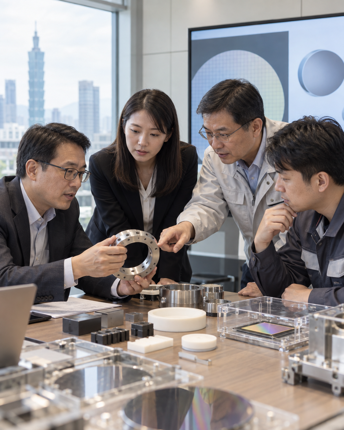
Baipu is connected to TSMC’s cutting-edge semiconductor manufacturing hub in the nearby Nanzih Technology Industrial Park. As Taiwan expands its semiconductor ecosystem—which had been concentrated in the north and central regions—to the south, it aims to establish not only manufacturing facilities but also capabilities in packaging, equipment, materials, testing, and talent development.
In Kaohsiung and southern Taiwan, companies such as ASE Technology and Foxconn are expanding their investments alongside TSMC. If Baipu operates as planned, advanced packaging and equipment verification capabilities—which follow wafer manufacturing—could be concentrated in the immediate vicinity, potentially reducing travel time and collaboration costs.
This agglomeration effect takes longer to achieve than a single company expanding its factory. Since research institutions, equipment manufacturers, materials companies, educational institutions, and skilled workers all need to be in place, the facility’s launch in 2029 is not the end but rather the starting point for building an ecosystem.
| You should continue to check the power status and construction schedule
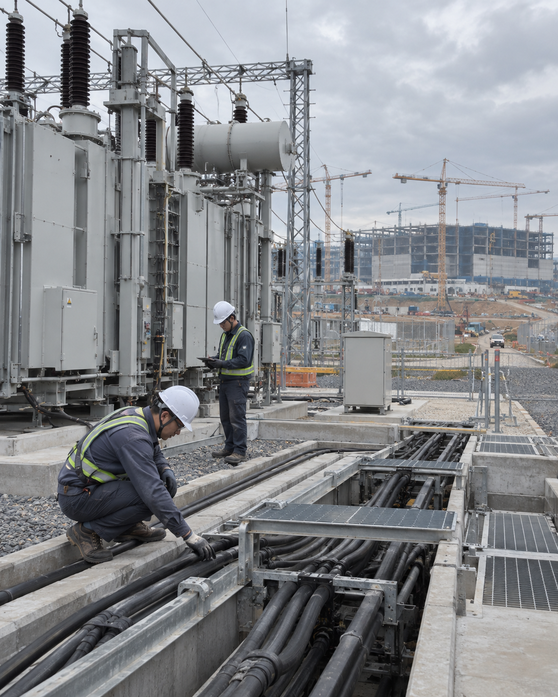
Semiconductor facilities for AI and high-performance computing require a stable supply of electricity and water, as well as logistics infrastructure. At the event, Taiwanese President Lai Ching-te reviewed electricity demand projections through 2035 and stated that there would be no issues with ensuring a stable supply. However, since these remarks were based on the government’s assessment and plans, the actual supply-and-demand situation and investments in the power grid must continue to be monitored.
The target of the fourth quarter of 2029 is also just a tentative date at this point. Actual operations can only begin once site preparation, building construction, equipment delivery, trial operations, and staffing are completed in that order. If there are construction delays or changes to the equipment delivery schedule, the start date for operations may also change.
Furthermore, while demand for advanced packaging is growing rapidly, the economic performance of industrial complexes cannot be guaranteed based on demand forecasts alone. Specific details regarding tenant agreements, the number of verifications, mass production adoption rates, and the number of jobs created must be disclosed in order to assess the effectiveness of the investment.
| The Significance of This Groundbreaking
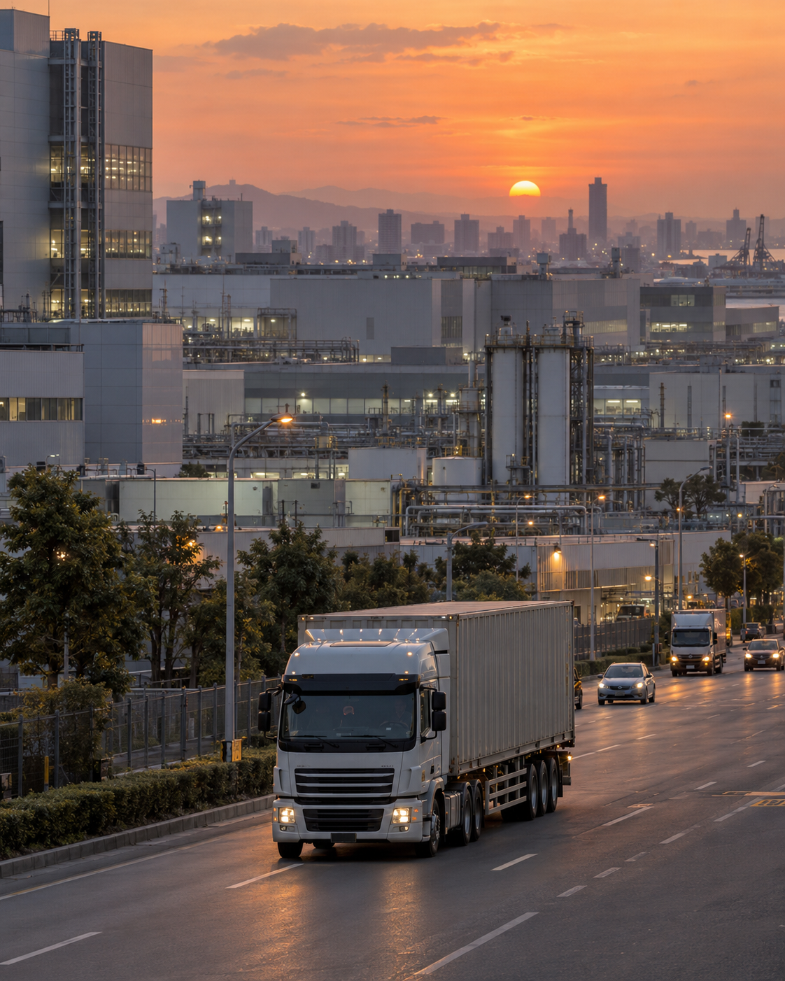
The key to this groundbreaking is The point is that Taiwan isn't just trying to maintain its competitiveness in advanced packaging by expanding production capacity alone, but has begun to integrate equipment and materials verification, as well as talent development, into a single regional ecosystem. This is a response aimed at accelerating the development of the supply chain as the bottleneck affecting the performance and supply of AI semiconductors shifts to packaging.
The confirmed details include the groundbreaking of the Baipu Industrial Park, its total area of approximately 88.7 hectares, plans for two TSMC facilities, and the target to begin operations in the fourth quarter of 2029. Specific details regarding tenant companies, investment amounts, production capacity, and technologies to be validated will be announced at a later date.
Going forward, we need to monitor whether construction progress, power and water infrastructure, the status of supplier move-ins, and actual verification results lead to mass production adoption. Only once these indicators are confirmed can we conclude that Baipu has evolved from a symbolic industrial complex into a substantive hub for southern Taiwan’s high-tech packaging supply chain.
References
Tags
#Taiwan #Kaohsiung #Baipu Industrial Park #TSMC #Advanced Packaging #AI Semiconductors #High-Performance Computing #Semiconductor Equipment #Semiconductor Materials #Semiconductor Supply Chain #Data Center #Semiconductor Infrastructure