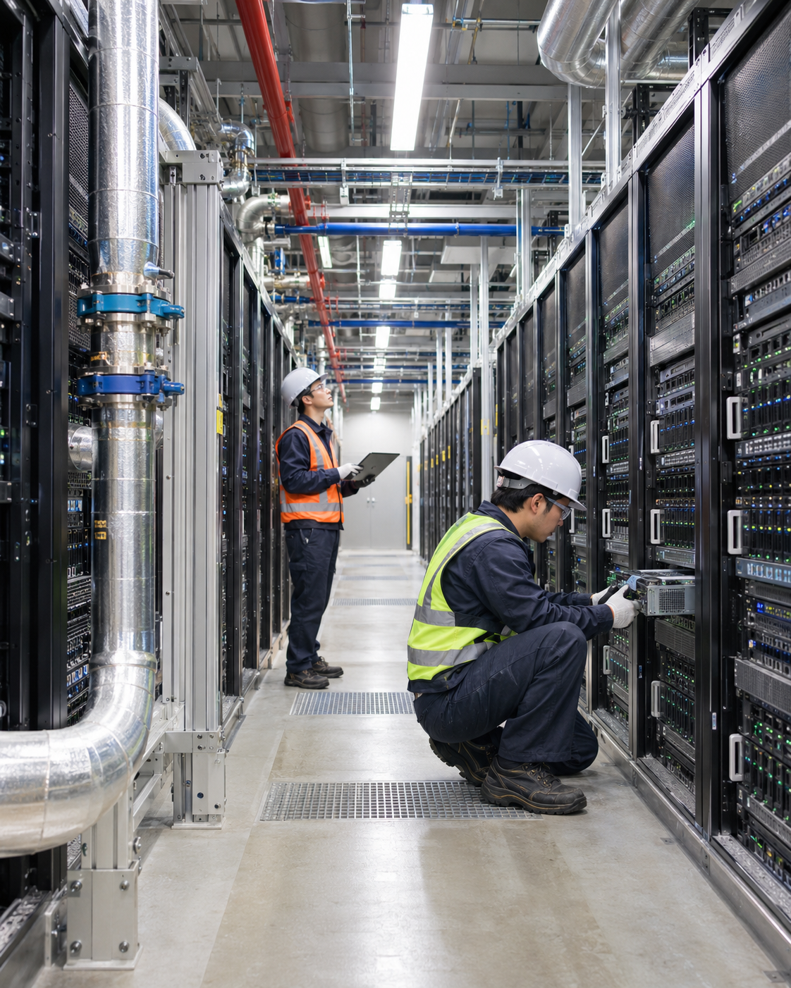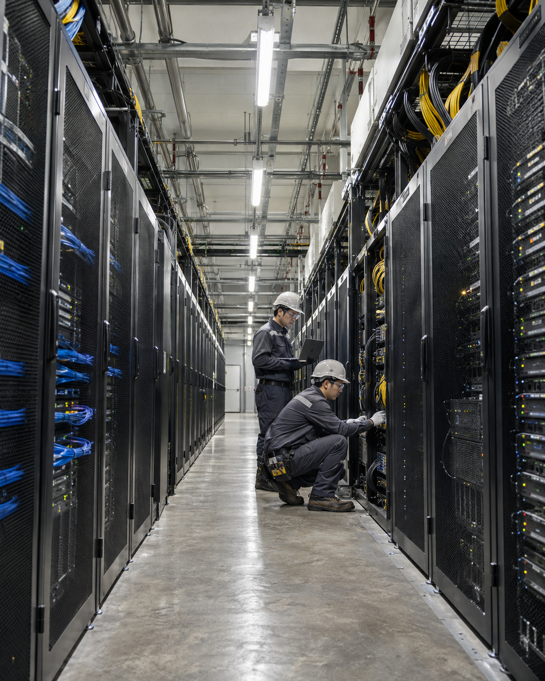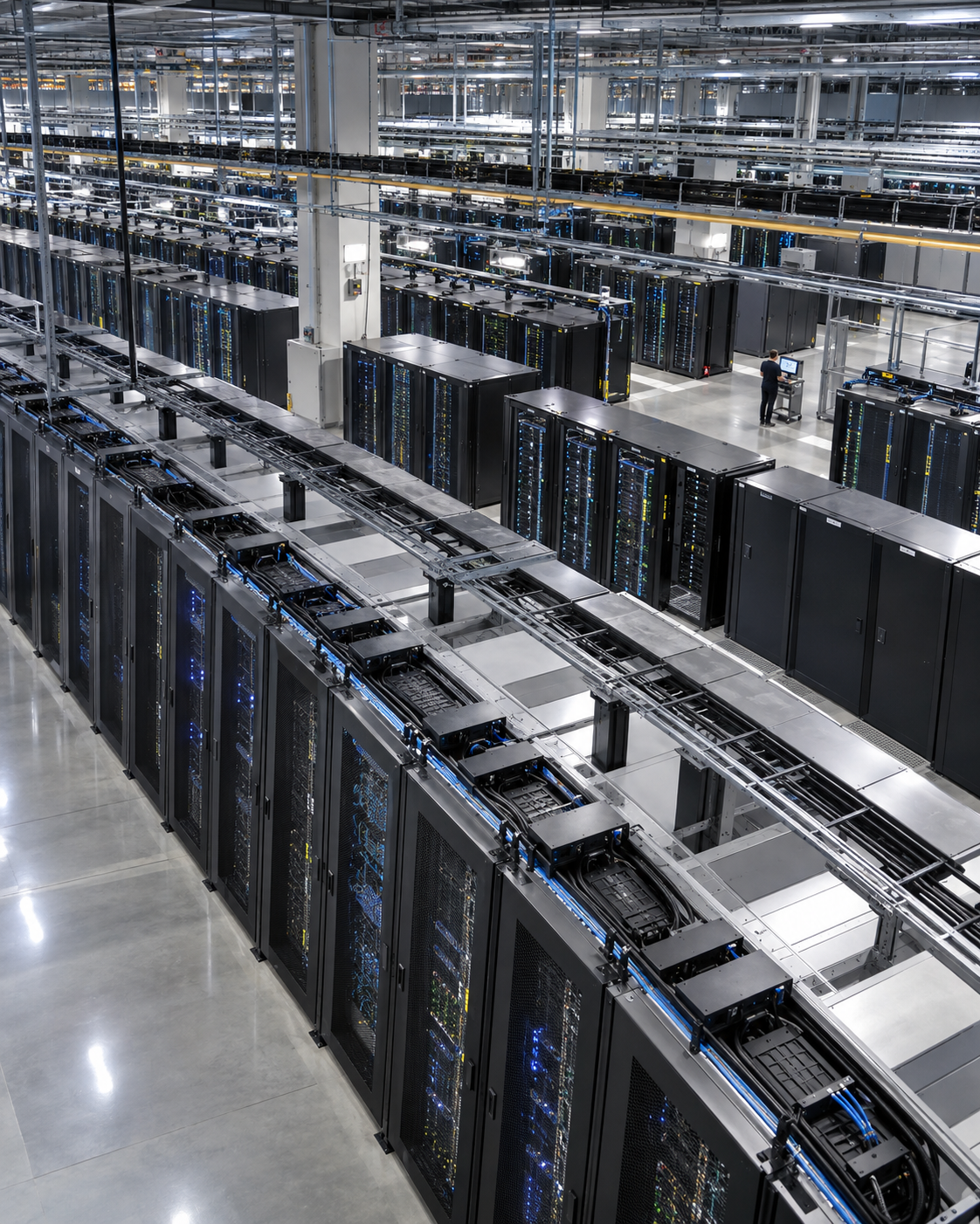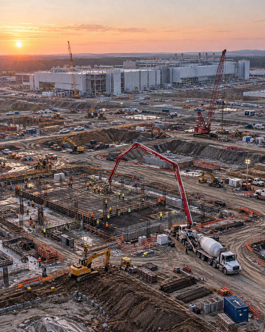
The company that will be responsible for the actual operations of a U.S.-Japan joint venture—worth up to $21 billion—to build two semiconductor factories in New York State has been selected. On October 14, GlobalFoundries (GF), a U.S. semiconductor foundry, announced that it had been selected as the technology provider and operator for the Malta, New York, site.
The most important word to keep in mind when reading this announcement is “maximum.” Just because the announced scale is large doesn't mean construction has started immediately at both plants or that the $21 billion has already been spent. We are starting the project with the first plant, and the decision regarding the second facility will be made separately at a later stage.
While cutting-edge computing chips tend to get all the attention in AI semiconductor news, a stable supply of basic semiconductors used in automobiles, industrial equipment, and telecommunications equipment is also crucial. This initiative can be seen as a move to further strengthen the production infrastructure within the United States.
| Up to $21 billion: What Has Been Decided?
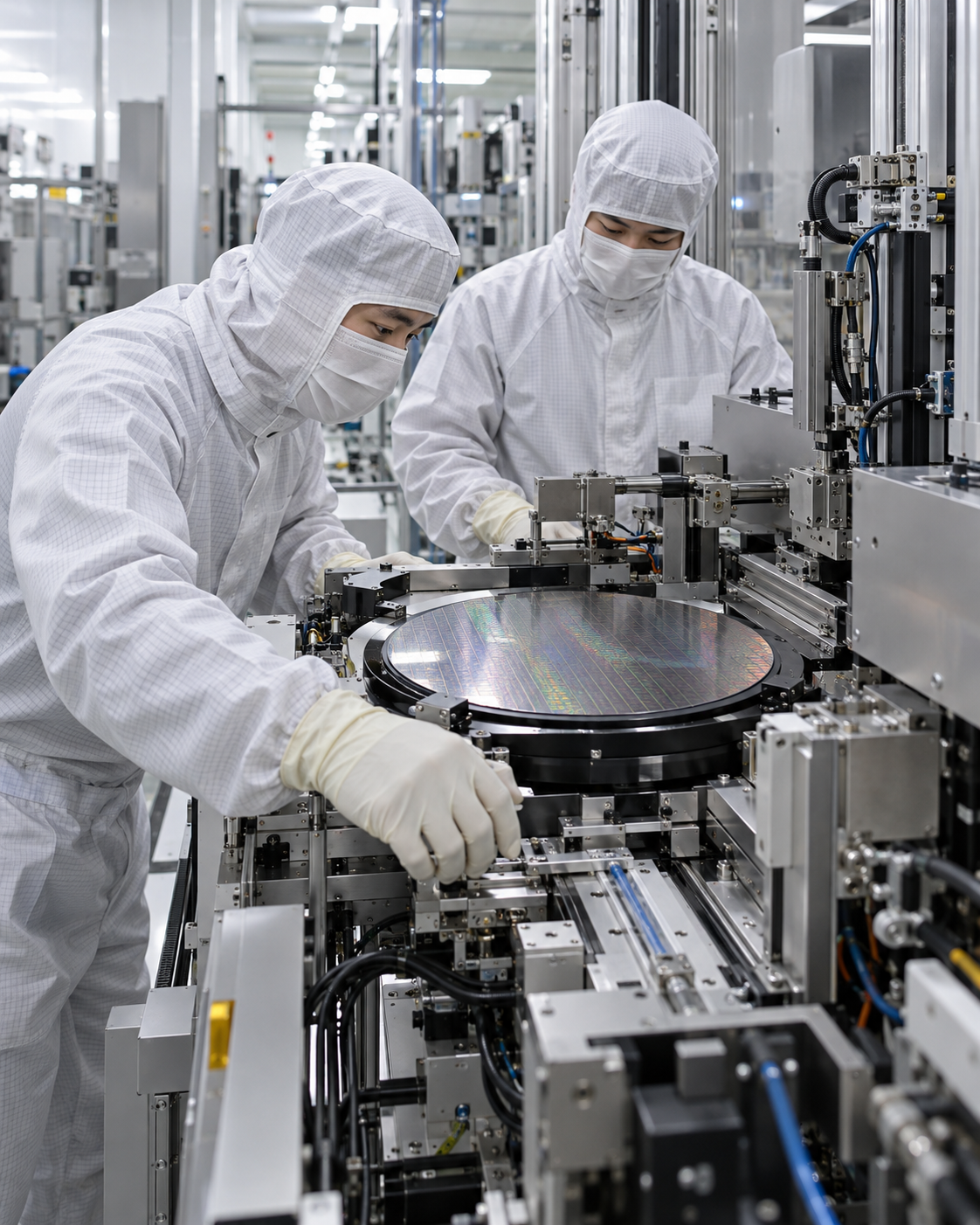
According to an official announcement by GF, the company has been selected to provide technology and oversee operations for two 300mm wafer fabs in Malta, New York, as part of a joint venture between the U.S. and Japan. Under this arrangement, Japan will provide the investment capital, while GF will be responsible for process technology and manufacturing and operational capabilities.
The key difference from previous investment plans is that we’ve designated an operating entity that will actually be responsible for the long-term tasks required until the factory is completed—such as design, securing personnel, bringing in equipment, and obtaining client certifications. However, being “selected as the operator” does not mean that the “factory will be completed” or that “all investments will be executed.” It is important to distinguish between the investment cap and the decision-making processes at each stage.
| Construction of the first plant is scheduled to begin in 2026, with production set to begin in 2029
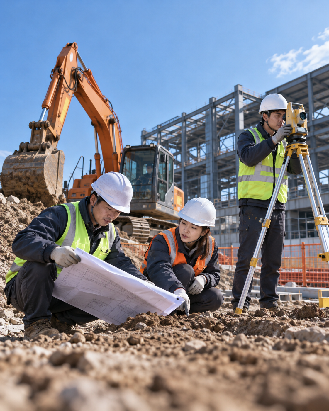
An initial investment of approximately $10 billion is set to be allocated to the first plant. GF plans to begin construction by 2026 by leveraging Malta’s existing infrastructure and permits, and has set a target of starting production in 2029. The advantage of this approach is that it is easier to integrate into the existing manufacturing ecosystem than securing a new site from scratch.
However, even if the target for breaking ground is met, we still need to secure yield rates and pass our customers’ quality inspections before we can achieve a production volume that allows for stable sales. 2029 is the schedule currently proposed by the company; it is not a definitive result where production and shipments are already guaranteed.
| What an annual production capacity of 900,000 wafers means
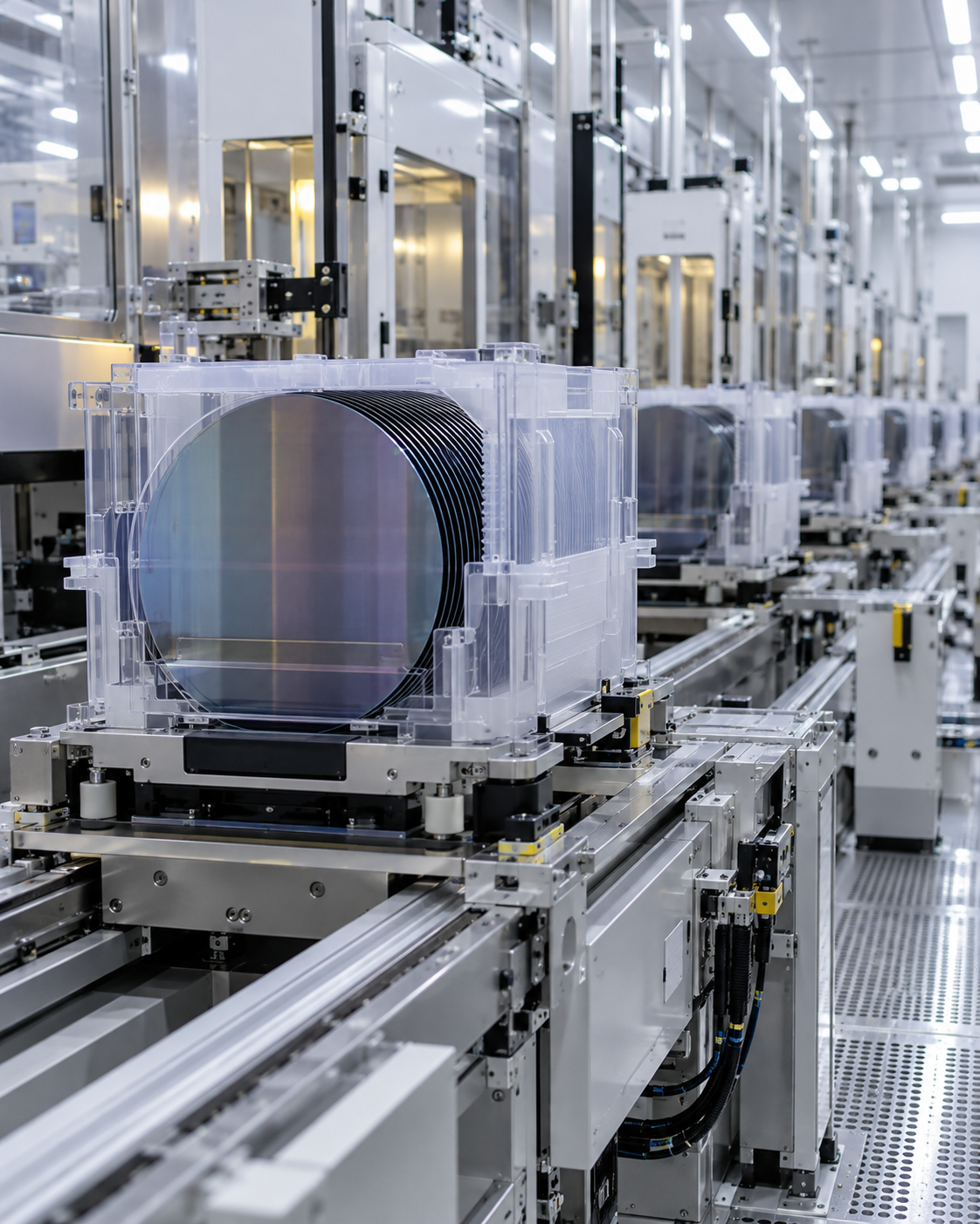
According to the company's estimates, once the first factory is fully operational, it will add an annual processing capacity of approximately 900,000 300mm wafers. If the second factory is actually built, it is said to add a similar capacity. A wafer is a circular silicon disc used to manufacture multiple semiconductor chips at once.
Although the annual wafer volume indicates a factory’s production capacity, it does not correspond directly to the number of finished chips or market revenue. The actual supply varies depending on the specific products being manufactured, as well as chip area and yield rates. Therefore, it would be misleading to interpret this figure as meaning that 900,000 wafers of all types of semiconductors are produced.
| The second factory and the investment funds are conditional
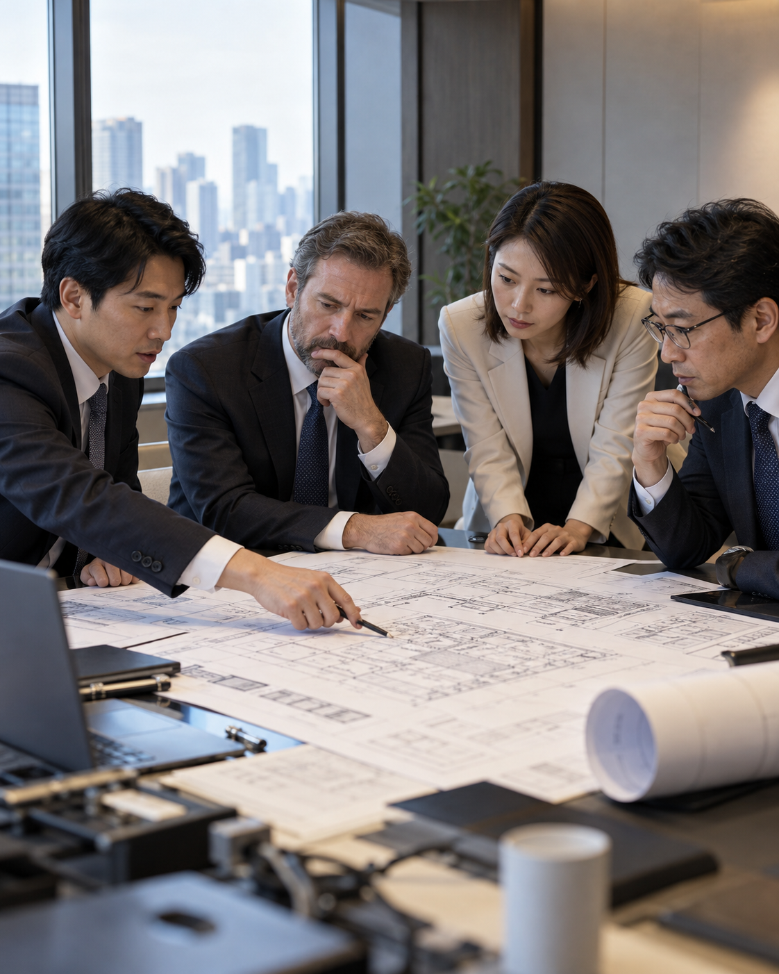
Although an additional investment of approximately $10 billion for a second plant is included in the plan, a final decision on construction has yet to be made. According to Reuters, the parties involved plan to decide by the end of 2028 whether to proceed with the second plant.
That’s why we need to distinguish between announcing the scale of investment and approving construction. Factors such as semiconductor demand forecasts, investment profitability, facility construction costs, equipment delivery schedules, and workforce availability can all influence the decision. Rather than writing “Construction of two plants confirmed” in the headline, it’s more accurate to maintain the conditional phrasing “planning to build up to two plants.”
| Expansion of the U.S. Government's Stake and Adjustments to Existing Subsidies
GF announced that it will receive approximately 4% of the company’s shares under a separate agreement with the U.S. Department of Commerce. Reuters reported that, when added to the U.S. government’s existing stake of about 3%, this brings the total to approximately 7%. In addition, GF has decided to reallocate $955 million from its existing CHIPS Act funding to accelerate investments in silicon photonics, silicon germanium, and advanced packaging in Malta, New York, and Burlington, Vermont.
The key point here is that investing in a new factory and reallocating existing subsidies are two distinct measures. The government’s equity participation also carries policy implications that differ from those of typical commercial investments.
| Why Is Semiconductor Production—Beyond Cutting-Edge GPUs—Also Important?
The product lines GF focuses on are used in a variety of fields, including automotive control, industrial equipment, connectivity, and telecommunications infrastructure. AI data centers also require various types of chips for power management, signal processing, and communication connectivity. Even if the number of cutting-edge computing chips increases, a shortage of semiconductors that handle peripheral functions could delay the production of the entire system. This is why the U.S. is seeking to expand its domestic manufacturing options for these products—to mitigate supply chain risks. You could interpret this as a way to keep costs down. That doesn't mean, however, that this factory will immediately become a state-of-the-art GPU production facility.
The economic impact of a semiconductor plant project isn't determined solely by the location where the plant is built and its size. It’s important to know how long a customer will continue to purchase the product, what production process they’ll adopt, and how reliably they’ll produce it. Because semiconductor manufacturers face high capital expenditures for equipment and the certification process with customers takes time, it may be difficult to convert the full production capacity into actual revenue immediately after a factory is completed. The automotive and industrial semiconductor sectors are areas where reliability—ensuring a consistent level of quality over the long term—is crucial. Once customer mass-production certifications and the product portfolio are disclosed, we’ll be able to evaluate the results of this investment more accurately.
| The Combination of Japanese Capital and U.S. Manufacturing Facilities
This project has a unique structure in that it combines Japanese funding, a U.S.-based factory, and GF's technology and operational capabilities. Japan is participating as a financier under a trade and investment agreement with the U.S., while the U.S. is working to expand its major semiconductor manufacturing base and create jobs. GF’s announcement also included statements from supply chain partners such as Renesas, Tokyo Electron, Apple, and Cirrus Logic. However, the fact that these stakeholders expressed support for the project does not necessarily mean that specific chip purchase volumes for the new factory or long-term supply contracts have been disclosed. Investment and purchase agreements are separate matters. That's the target.
Furthermore, while the announcement of a new plant points to the potential for expanded local employment, it is important to distinguish between the company’s estimates for construction and ecosystem-related jobs and the actual number of long-term employees. This is because the temporary labor demand during the construction period differs from the specialized manufacturing workforce needed once production begins. The economic impact on the region is expected to become clear as the project progresses.
| Three Milestones We'll Explore Next
First, whether actual construction will begin in 2026 and on-site work will proceed as planned. Second, whether equipment installation and customer certification can be completed by the 2029 target date. Third, whether a final investment decision on the second plant will be made by the end of 2028. If the product mix for each process and stable yield rates are also disclosed, we’ll be able to evaluate the business’s value more accurately. The achievements at this stage involve turning a large-scale investment plan into a concrete operational entity and the first business This means they've aligned their schedules, but the remaining challenge is that their future production capacity has not yet been confirmed through actual wafer shipments.
Tags
#GlobalFoundries #GlobalFoundries #U.S. Semiconductors #Investing in Japan #Semiconductor Factory #NewYorkMalta #Semiconductor Supply Chain #Foundry #300mm Wafer #CHIPS Act #U.S.-Japan Cooperation