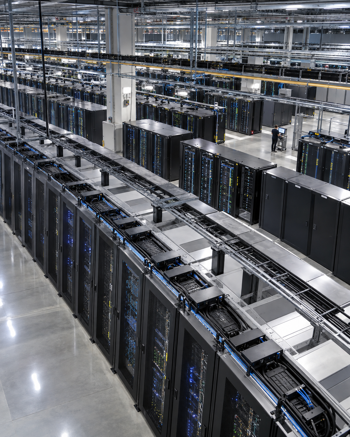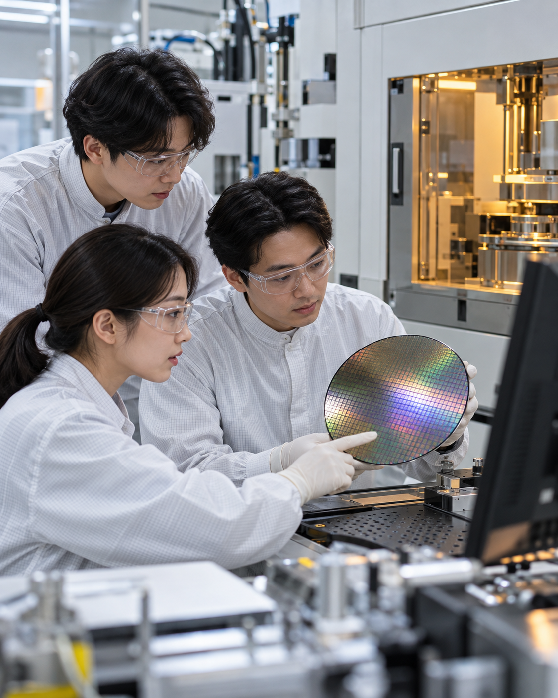
The semiconductor industry is moving beyond the production of AI chips to, There is a growing trend toward utilizing AI in the process of designing and manufacturing semiconductors. On October 14, NVIDIA unveiled the CUDA-X libraries—designed for semiconductor design, manufacturing, and testing—along with use cases from its partners in an official announcement.
The figures provided by the company are particularly striking. The new cuPotential accelerated existing GPU-optimized tasks by an additional 2 to 3 times in initial tests, and included cases where it potentially accelerated specific Synopsys simulations by up to 30 times and Applied Materials’ chamber simulations by up to 35 times.
However, it’s problematic to treat numbers from different tests as if they represent a single, common performance metric. To truly understand the real changes in AI-based semiconductor manufacturing, we need to distinguish which software performed which calculations and how quickly, as well as how far the actual field implementation has progressed.
| What Kind of Factory Is an "AI-Defined Fab"?
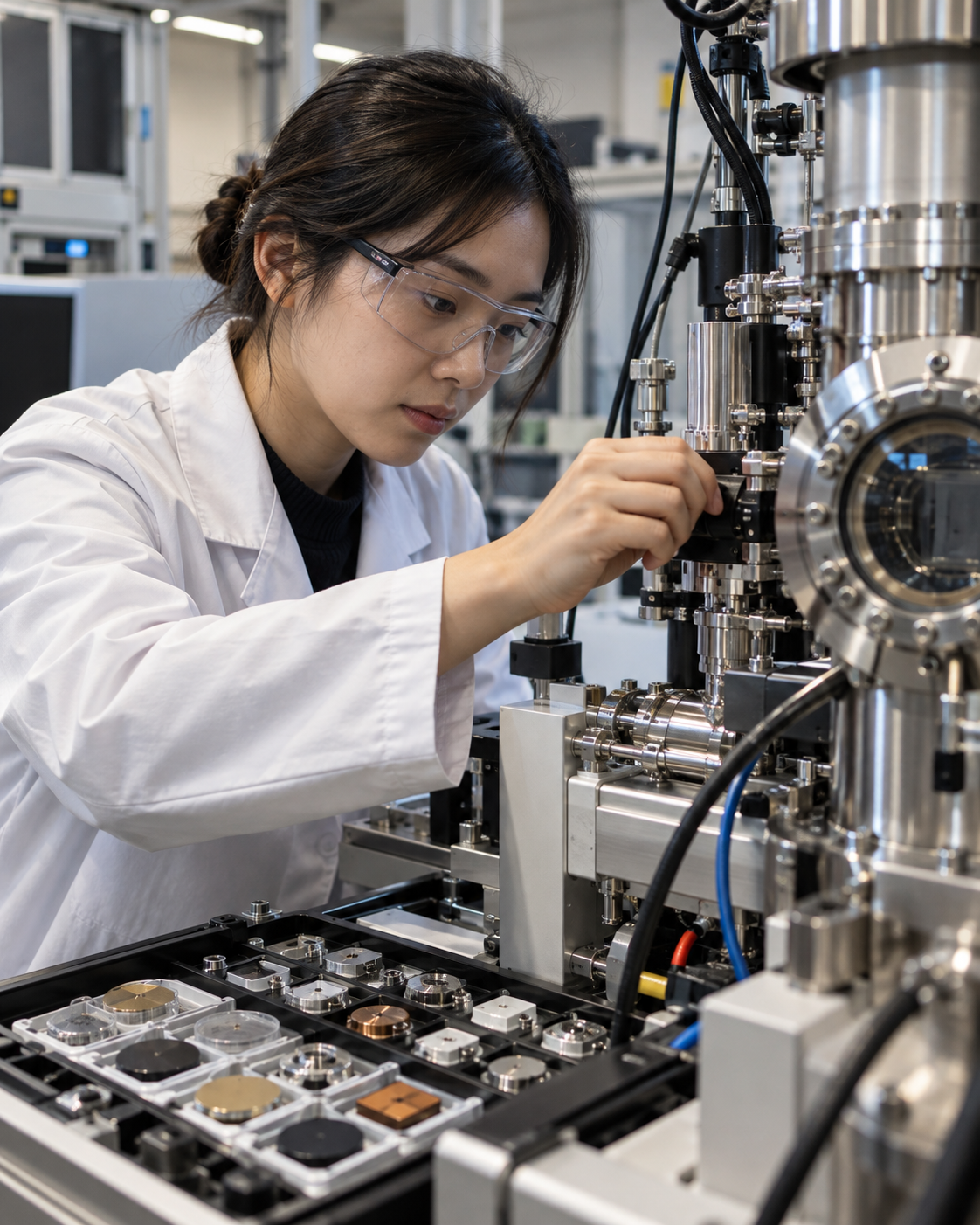
The term "AI-defined fab," as used by NVIDIA, refers to a semiconductor manufacturing facility where artificial intelligence supports process analysis, equipment operation, quality inspection, and the resolution of production issues. Semiconductor factories have long made extensive use of automation and statistical process control.
The shift is toward connecting simulation and data analysis capabilities so that AI agents can access and iterate on them more easily. For example, when testing new material combinations or analyzing equipment conditions, instead of humans performing every calculation step manually, the software can take over some of the tasks. That doesn’t mean we’ve immediately achieved a fully automated factory where humans are no longer needed.
| The Role of the New cuPotential Library
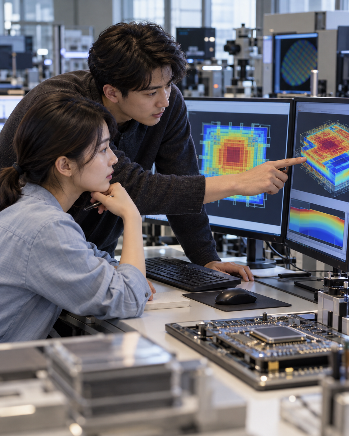
cuPotential provides the GPU acceleration needed to calculate the forces and interactions between atoms and molecules. In semiconductor manufacturing processes, these calculations are important for understanding the properties and reactions of materials.
According to NVIDIA, in initial pilot tests, it has already accelerated workflows that were already optimized for GPUs by an additional 2 to 3 times. The key point here is that the benchmark is not “existing CPU workloads” but “workloads already optimized for GPUs.” Additionally, cuPotential is available as an early access release at the time of this announcement. It should not be interpreted as a full-scale, general-purpose release that guarantees the same performance for everyone in every environment right away.
| Case studies showing up to 30-fold improvements, as published by Synopsys
NVIDIA noted that Synopsys uses cuPotential, cuEST, cuDSS, and other tools for semiconductor simulation. According to specific figures from the company’s announcement, initial results using cuEST with QuantumATK showed a potential 30-fold speedup, while the cuDSS benchmark for S-Device indicated a 12-fold speedup.
Therefore, stating that “a single cuPotential made the entire Synopsys process 30 times faster” would be an inaccurate description. The results should be broken down by calculation type and software. Synopsys also introduced an approach that connects AI agents for design and verification with NVIDIA’s Nemotron and NeMo technologies.
| The Difference Between Lam Research and Applied Materials
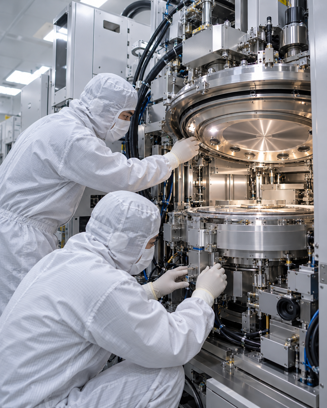
Lam Research plans to integrate NanoVDB, an open-source library for 3D data processing, into its semiconductor process modeling platform, SEMulator3D. The company announced that it aims to achieve up to a 30-fold speedup in certain wafer etching simulations and plans to release the related features by the end of 2026.
In contrast, Applied Materials’ figure of up to 35x is based on chamber simulations using NVIDIA Omniverse and CUDA-X. The specific tasks and deployment conditions are different. It’s important to distinguish between technologies already in use in the field, test results, and future release goals.
| GPU Technology Is Also Gaining Ground in the Inspection and Quality Assurance Fields
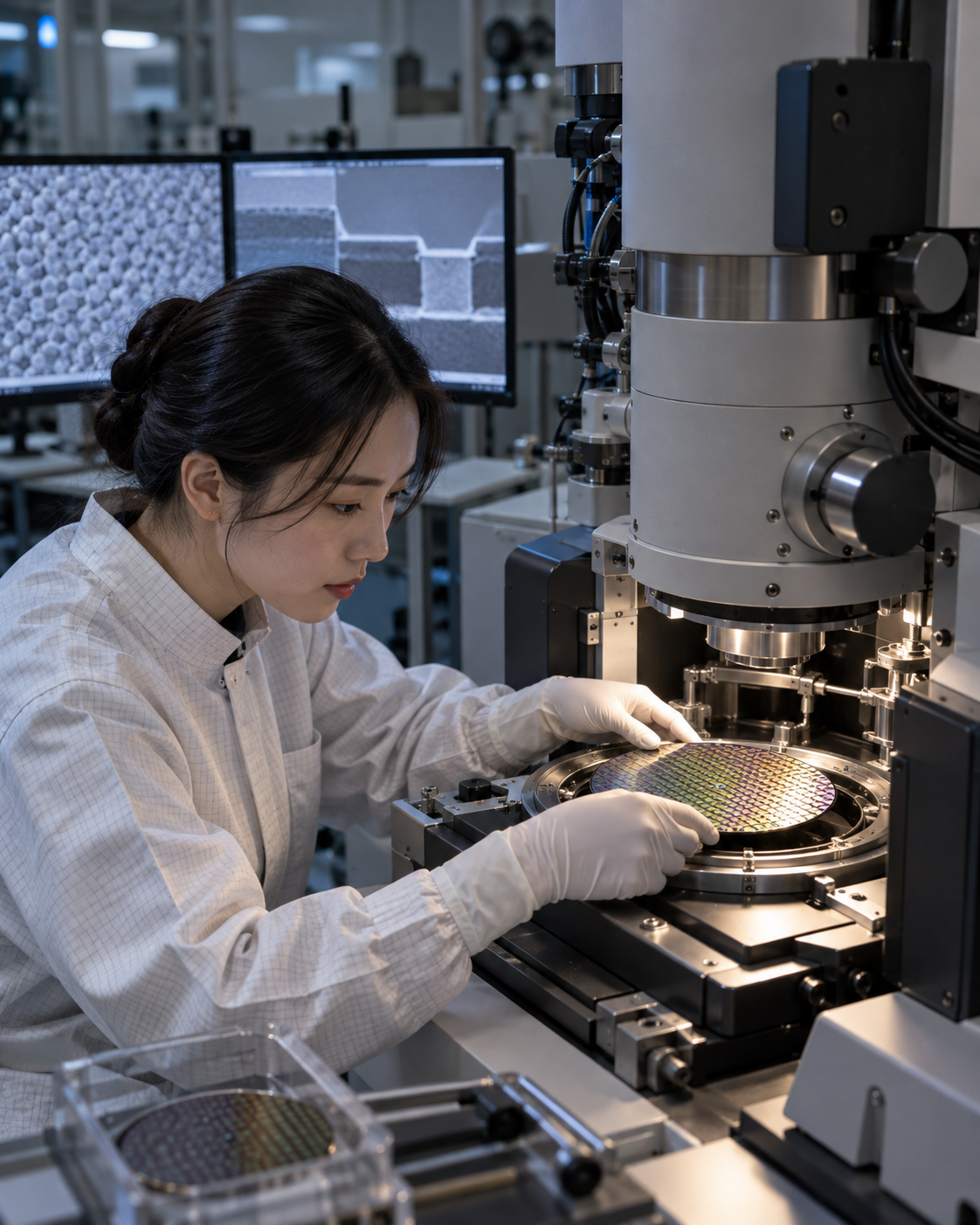
In the manufacturing industry, process simulation isn’t the only task where speed matters. Comparing the vast number of images captured by inspection equipment to detect defects also requires significant computational power. NVIDIA explained that KLA confirmed the NPP-based system for image processing delivers performance up to 50 times faster than the previous CPU-based version.
Teradyne reported an approximately 85-fold performance improvement in probe maintenance analysis, while imec presented results on improvements to the lithography process window. While these results demonstrate the potential for improved production efficiency, their true value can only be assessed by also verifying the accuracy of the inspections and whether any false defect calls were made.
| Where Design Automation Meets Physical Simulation
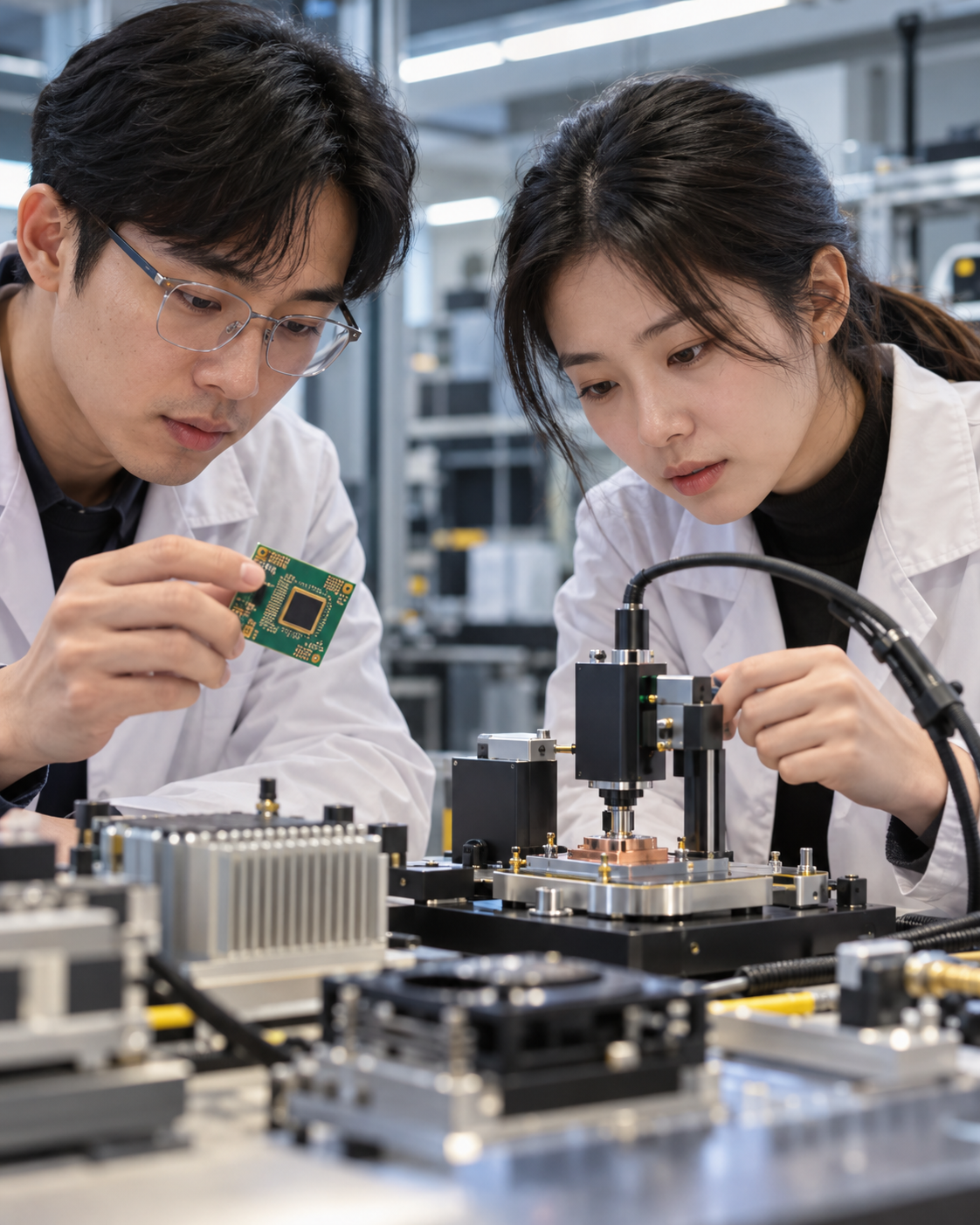
Cadence has unveiled a case study demonstrating how AI agents and GPU-accelerated solvers can rapidly perform thermal and stress analysis for advanced packaging, while Siemens is working to automate circuit pattern correction and model characterization. Semiconductor design must take into account not only electrical characteristics but also heat generation, structural deformation, and material reactions.
If software that calculates different physical domains is integrated, there is potential to reduce the time spent on the iterative process of testing and revising design proposals. However, there is a world of difference between “support for design automation” and the claim that “AI independently designed an entire chip and brought it into mass production.”
The biggest advantage of faster simulation speeds is that it allows us to test more design hypotheses in the same amount of time. However, even if the calculations are fast, the predictions may be inaccurate if they don't match actual semiconductor manufacturing conditions.
Models used to predict the physical behavior of materials or equipment may become increasingly inaccurate when used beyond their validated range. Rather than immediately applying process changes recommended by AI agents to mass production facilities, it is necessary to follow a procedure that includes expert review and small-scale experiments. Improvements in speed and verification of manufacturing quality must go hand in hand.
| The figure "30 times" doesn't mean 30 times the factory's production volume.
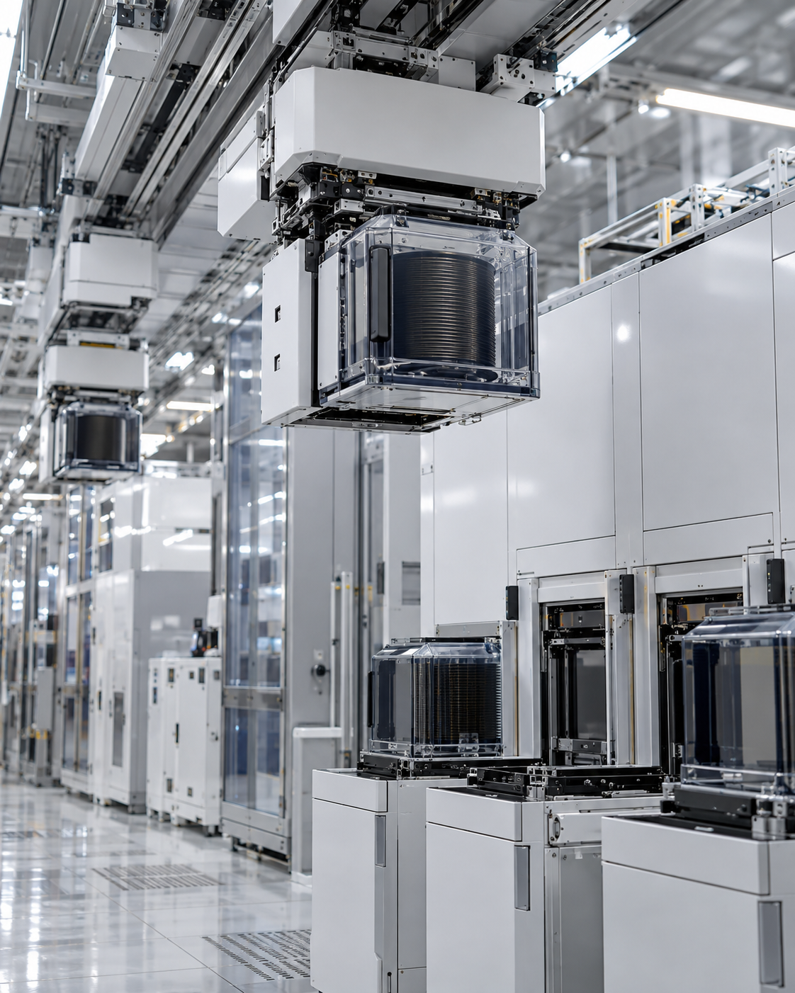
Benchmark results vary depending on specific input data, hardware configurations, software versions, and measurement methods. Even if you run a single step of the simulation 30 times faster, the total chip production time isn't reduced by the same proportion. That's because other steps—such as raw material processing, equipment setup, exposure, etching, inspection, and rework—still remain.
Furthermore, even if AI predictions become faster, changing actual process conditions requires verification and approval procedures. Therefore, we should avoid presenting the figures in this announcement as if they represented a 30- to 35-fold increase in factory yield or finished product output.
| The key to scaling up lies in reproducibility and actual manufacturing performance
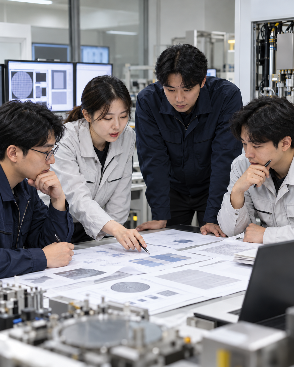
This announcement signals that NVIDIA's computing platform is becoming more deeply integrated into semiconductor companies' design and manufacturing software. The company is currently offering cuPotential on a limited basis; some partners have shared use cases, and other features are slated for future release.
The next metrics to examine are whether similar speeds can be replicated in an independent environment, whether design schedules and defect analysis times are actually shortened, and what impact this has on costs and yield. While the use of AI to assist in semiconductor production is expanding, the measured acceleration performance and verified factory operational results are not yet on the same level.
Tags
#NVIDIA #NVIDIA #CUDA_X #cuPotential #Semiconductor Design #Semiconductor Manufacturing #AI Agent #Semiconductor Simulation #Synopsys #AppliedMaterials #LamResearch #AI Factory